콘텐츠로 건너뛰기
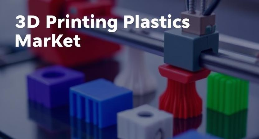
3D printing technology has rapidly evolved in recent years which allowed manufacturers to deposit materials to form objects in real life from trails. Originally 3D printing tool for developing prototypes for manufacturing designs and plastics sectors and parts, researchers and engineers are now using it for complex application like printed wiring. Based on the additive manufacturing known as 3D printing, printed electronics or the layering of circuitry circuits and electronic components to produce workable electronic systems. This new technique opens the door for new design solutions in electronics manufacturing that have not been possible with previous techniques.
Curing and sintering or sintering of conductive and non-conductive materials deposited layer by layer in the exact patterns means that any number of-functions explored in 3D printing can be incorporated, from circuits, antennas, and sensors and many others. One of the benefits of 3D printed electronics to on-demand customization of a given electronic product is made possible. In the aspects of both circuit board layout and wearing device, it reduced the cost of complexity integration, and can be quickly designed, tested and produced.
This mass customization capability opens up new possibilities for Internet of Things devices, medical implants, consumer electronics and other industries where personalized or low-volume products are needed. Precision tissue scaffolds, biosensors and smart medical implants are especially well-suited for additive circuitry techniques.
Several key materials technologies have enabled significant progress in 3D printed electronics. Conductive inks made from silver, gold and carbon nanotubes allow intricate patterns of electrical pathways to be deposited with high resolution 3D printers. Dielectric and insulating inks are also available to effectively separate and encapsulate conductive traces. Combined with developments in multi-material 3D printing heads and multi-nozzle extruders, these inks facilitate the layer-by-layer fabrication of functioning circuits and devices.
The integration of surface mount electronic components like resistors, capacitors and integrated circuits directly into 3D printed structures brings printed electronics one step closer to fully replacing traditional manufacturing. Using pick-and-place robotics, these passive and active electronic components can now be automatically positioned and secured during or after the printing process. This opens up possibilities for true system-level printing with embedded computation, sensing and wireless connectivity.
Moving forward, printed electronics researchers are striving to improve conductivity, resolution and yield through new materials formulations and 3D printing process innovations. Combined multi-axis printing, curing methods and online quality control will likely yield finished electronic products withperformance matching traditionally manufactured circuits. Additional work on in-nozzle sensing, closed-loop process control and refinement of multi-materials handling promises to optimize resin 3D printing circuits and smart product design. Progress in these areas means the digital fabrication of fully-functional electronic devices through additive manufacturing is becoming increasingly viable.
In summary, 3D printed electronics is an evolving and promising field that blurs the boundaries between manufacturing and design. By integrating additive design freedom with functional circuitry fabrication, it enables unprecedented possibilities for customized electronic products tailored to niche applications and personalized needs. Continued materials and process advancements will drive 3D printed electronics towards mainstream commercialization and adoption across many industries in the coming years.
Multi-material 3D Printed Electronics
Fabricating Hybrid Circuits with Different Materials
Modern multi-material 3D printers allow the simultaneous deposition of both conductive and non-conductive materials. This enables:
- Fabricating complex electronic components from different materials in a single print, such as metals, conductive polymers and insulators.
- Producing hybrid circuits containing integrated electrical and mechanical parts without additional assembly steps.
- Conformal circuit designs that can be embedded within non-planar 3D structures.
Embedded Electronics
Recent research has demonstrated techniques for embedding wires, chips and other electronic components directly into 3D printed thermoplastics during the fabrication process. This allows functional circuits to be integrated within complex 3D geometries.
Filament-based Methods
Filament-based 3D printers first deposit an insulator material then selectively print conductive traces using specialized filaments. Researchers have developed new conductive polymer filaments for this approach.
Functional Inks for Printed Circuitry
Silver Nanoparticle Inks
Silver nanoparticle inks offer high conductivity and resolution. They are commonly 3D 프린팅 사용 in aerosol jet, inkjet and extrusion printing of flexible and printed electronics. Traces produced from these inks can rival the performance of traditionally manufactured copper circuits.
Graphene/Carbon Inks
Graphene and carbon inks produce inexpensive, lightweight conductive traces. They find applications in bendable touchscreens, wearables and bioelectronics due to their mechanical flexibility. However, conductivity is typically lower than silver inks. New formulations aim to improve this for circuit applications.
Hybrid Circuits
To overcome limitations of single-material approaches, researchers are integrating 3D printing with traditional lithography. Some approaches print conductive traces onto custom 3D substrates that are later processed using established lithographic techniques. Others embed 3D printed electrical components as one layer into multi-layer hybrid circuits fabricated using both additive and subtractive methods. This expands the complexity of printable circuits beyond what is currently achievable with 3D printing alone.
Advances in 3D Circuit Fabrication
Higher Resolution Printing
Technological improvements have boosted 3D printed electronics capabilities. Higher resolution 3D printers can now deposit finer conductive traces measuring below 100 microns. This enables more dense and sophisticated circuit designs.
Embedded Electronics
New techniques integrate active devices like chips, sensors and energy storage components directly within thermoplastic substrates during 3D printing. This allows production of fully-functional electronic systems with no post-processing required.
Multi-Nozzle Printing
Multi-nozzle 3D printing systems can deposit different functional materials simultaneously for improved registration between components and increased yields. Insulators, conductors and active 3D 프린팅 재료 can be placed precisely.
Flexible and Stretchable Conductors
Processing innovations help produce stretchable and self-healable conductors enabling flexible and wearable 3D printed electronics. Circuit designs can now bend, stretch and potentially recover from damage.
Passive Component Integration
Embedded 3D printed waveguides, antennas and other passive components enable compact wireless circuits and Internet-of-Things devices to be produced additively. This expands design possibilities for printed electronics.
Applications and Future Trends
Wearables and Implantable
3D conformal circuits enable seamless integration of electronics into apparel, prosthetics and implantable medical devices through additive circuit designs.
Smart Objects and IoT
Embedding intelligence and connectivity using 3D printed electronics allows new generations of interactive products, home automation systems and industrial sensors to be developed.
Microfluidics and Bioelectronics
3D printing allows the integration of electronic components with fluidic channels, valves and reactors for applications in chemical analysis, organ-on-a-chip development and personalized medicine.
Aeronautics and Space Technologies
Conformal printed circuits permit lightweight, ruggedized avionics, satellites and ground support systems optimized for advanced applications in avionics and aerospace.
Advancing Technologies
Research is improving multi-material techniques, achieving nanoscale printing precision, developing new self-assembly methods and exploring hybrid manufacturing approaches to realize even more sophisticated 3D printed electronic systems. The field is poised to revolutionize electronics manufacturing.
결론
3D printed electronics has seen tremendous advancements in recent years and is positioned to drastically impact various industries going forward. Material innovations have enabled viable printed conductors and dielectric inks, while multimaterial printing now routinely embeds both passive and active electronic components within complex 3D geometries.
These technologies allow completely customized and conformal circuits impossible to produce until now. From medical devices to consumer products to aerospace engineering, any application involving specialized electronic enclosures or one-off designs is a candidate for digital additive manufacturing. As techniques mature, 3D printed electronics will continue integrating more closely with traditional lithographic processing to achieve system-level solutions.
Resolutions under 100 microns now easily surpass many conventional PCB fabrication capabilities. Adoption of 3D printed circuitry will accelerate as yields increase and 3D Printer Cost decrease through ongoing process refinements. The ability to mass-customize at reduced volumes makes additive manufacturing particularly compelling for IoT and personalized medicine. Further expanding applications in flexible and bioelectronics will drive continued innovation in materials sets and printing approaches.
Within this decade, 3D printed electronics is expected to supplant traditional production methods for many compact and complex circuit applications. As multi-material additive techniques evolve to industrial maturity, digital manufacturing will transform electronic product development and customize devices at scale. 3D printing’s design freedoms and integrated functionality pave the way for next-generation smart networked devices.
자주 묻는 질문
Q: How does 3D printed electronics differ from traditional manufacturing?
A: It uses additive processes to directly fabricate circuits layer-by-layer rather than subtractive etching and assembly. This enables novel designs like embedded/conformal circuits and ease of customization.
Q: 일반적으로 어떤 재료가 사용되나요?
A: Silver, carbon and polymer-based inks provide conductive traces while plastics like thermoplastics act as dielectric insulators between traces. Advances in nanomaterials and inks are expanding the library of printables.
Q: How accurate can traces be?
A: Leading technologies can print lines as fine as 50 microns with high resolution extrusion and aerosol jet. Registered multimaterial printing further increases density.
Q: When will it surpass conventional PCBs?
A: Mass customization advantages already serve niche markets. But yields must still improve for cost/performance parity needed for high-volume consumer applications within 5-10 years.